Research
Highlights...
 
 
Jacek Sekutowicz

Jacek Sekutowicz

 
See below


 Number 140 September 1, 2003 


SLAC makes shortest bunches in the world

To make never-before seen direct observations of atomic matter in motion, DOE's Stanford Linear Accelerator Center has made the world's shortest bunches of electrons: only 12 microns (millionths of a meter) long and 80 femtoseconds (one quadrillionth of a second) fast. During its first run this summer, the Sub-Picosecond Pulse Source (SPPS) made high current, ultra short bunches of electrons and turned them into very bright, ultra short pulses of X-ray light. These are the first X-rays made by a linear accelerator and are 1,000 times shorter than those made by storage rings (including SPEAR at SLAC). The gymnastics of rotating and compressing the bunches (which each contain 21 billion electrons) required advanced accelerator research and design and will be a crucial component of SLAC's future Linac Coherent Light Source.

[Neil Calder, 650/926-8707;
neil.calder@SLAC.Stanford.EDU]

JLab physicists study 'nothing'!

Vacuum
Vacuum

New measurements taken using the DOE's Jefferson Lab CEBAF Large Acceptance Spectrometer are telling us more about how matter is produced from "nothing," that is, the vacuum. Matter and anti-matter can be created when energetic particles strike one another. The new particles are created from the available kinetic energy of the particles that collide. Physicists think the first step in the process is to produce a pair of quarks: one quark and one anti-quark. Like electrons and protons, quarks are thought to spin on their axes, like little tops; and they were expected to be produced with their spins lined up. However, the CLAS measurements indicate just the opposite! The quarks emerge with spins anti-aligned.

[Deborah Magaldi, 757/269-5102;
magaldi@jlab.org]

Sandia researchers learning from seashells, diatoms

nanocrystals
Complex nanostructed crystals have been prepared showing striking similarities with those observed in biominerals. (a) is nacre in red-abalone. (b) is synthetic ZnO crystals. (c) is a diatom. (d) to (h) are different types of synthetic silica crystals. The morphology depends on the growth conditions and can be controlled.
Researchers at DOE's Sandia National Laboratories are developing complex nanomaterials that look strikingly similar to the microstructures of diatoms - unicellular algae - and seashells. The materials may have potential for a wide range of applications including chemical and biological sensing and diagnosis, photovoltaic cells, hydrogen storage, drug delivery and optical storage. The researchers' goal is to develop general science and technology for reliable and scalable production of nanoscale materials based on environmentally benign chemical processes. The biochemical processes involved in biomaterials are too complicated for synthetic materials, so the team is learning from the physical and chemical principles behind the formation of natural materials, and is developing synthetic routes to achieve similar structural control.

[Howard Kercheval, 505/844-7842;
hckerch@sandia.gov]

Electricity on the spot

Combined Cooling, Heating, and Power (CHP) Integrated Laboratory
As a National User Test Facility, ORNL's Combined Cooling, Heating, and Power Integrated Laboratory supports research and development of energy-efficient distributed generation systems for business and industry.

Power blackouts need not interrupt normal routines such as keeping phone circuits and hotel electric systems operating. Using energy sources produced through the concept of distributed generation, Verizon Communications and a Hilton Hotel outside of Gary, Ind., may soon be able to operate regardless of whether these facilities are receiving electricity from the power grid. In tests coordinated by DOE's Oak Ridge National Laboratory, distributed generation produced on-site uses fuel cells, microturbines or natural gas-fired reciprocating engine electric systems to produce electricity. In addition, these systems use what would otherwise be waste heat to provide heating or cooling to the facilities, making greater use of the fuel energy.

[Fred Strohl, 865/574-4165;
strohlhf@ornl.gov]

Leading the way on superconducting radiofrequency cavity redesign

Jacek Sekutowicz
Jacek Sekutowicz

Jacek Sekutowicz, a visiting senior staff scientist at the DOE Jefferson Lab's Institute for Superconducting Radiofrequency Science and Technology in Newport News, Va., remembers when, as a high schooler in Warsaw, Poland, he became captivated by applied physics. "Accelerators were very interesting to me. It was fascinating to know you could move a particle almost at the speed of light," he says.

As he grew older, Sekutowicz amplified that interest, by getting a Master's in Microwave Electronics at Warsaw Technical University and a Master's in Mathematics at Warsaw University. In 1985, while working at the Institute for Nuclear Studies on medical accelerators, he had nearly completed a Ph.D. in physics when he received a job offer from DESY (the Deutsches Elektronen Synchrotron) in Hamburg. The degree was completed after he decided to stay in Germany. "I came to Hamburg for one year only. Now, 18 years later and I am still there," he adds.

As one of the world's experts in superconducting technology, Sekutowicz began collaborating with JLab a few years ago when the Lab started its work on the Spallation Neutron Source project. He is currently helping JLab design and refine the next generation of niobium cavities as part of a proposed 12 billion electron volt (12 GeV) upgrade to JLab's accelerator. The accelerator upgrade is the first step in a process that will enable JLab researchers to push beyond the frontiers where they now delve into quark-related physics.

Sekutowicz is participating in the design of new cavities and devices known as high order mode couplers, which he and his colleagues believe are needed to reduce or eliminate "parasitic" modes: electromagnetic oscillations set up by the accelerated beam as it passes through the cavities. These oscillations can, like the backwash of water in a storm-tossed bay cutting off the tops of wind-tossed waves, reflect back on the beam and degrade its quality.

Submitted by DOE's Jefferson Laboratory

DOE Pulse highlights work being done at the Department of Energy's national laboratories. DOE's laboratories house world-class facilities where more than 30,000 scientists and engineers perform cutting-edge research spanning DOE's science, energy, national security and environmental quality missions. DOE Pulse is distributed every two weeks. For more information, please contact Jeff Sherwood (jeff.sherwood
@hq.doe.gov
, 202-586-5806)

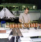
Unlocking metallic glass' mysteries

DOE's Ames Laboratory researchers Dan Sordelet and Matt Kramer are working to understand why metallic glasses take on various structures and properties depending on how the materials were processed.

Normally, metals have a very regular (periodic) structure in which the atoms align. This ordered arrangement contains damage mechanisms that allow crystalline metals to be permanently bent or dented. By definition, glass - including the common window variety - is formed when a material is synthesized in such a way that a regular crystalline structure isn't formed. This random, or amorphous, arrangement of atoms gives metallic "glass" the ability to snap back into its original shape instead of deforming - as long as it's not bent too far.

These fascinating materials have a number of unique physical and sometimes electrical and magnetic properties but are difficult to study because of the ways and speeds with which they form. The materials Sordelet and Kramer are studying have been melt-spun - a stream of molten metal is dropped onto a spinning copper wheel and solidifies in a ribbon before the atoms can line up. They are also looking at metallic glass formed by high-energy mechanical milling that destroys the crystal structure to such an extent that it becomes amorphous, and by laser deposition in which a laser vaporizes materials into highly energetic atoms that condense randomly in a thin coating.

With all of these contrasting synthesis methods, it's difficult or impossible to find out what's taking place at the atomic level as the amorphous structure forms. So the two researchers work backwards, in a way, through a process called devitrification. This involves gradually heating the metallic glass until it devitrifies - loses its amorphous properties - and the atoms realign in the metal's regular crystalline pattern.

"From a fundamental viewpoint, we want to try to make the linkage between the structure that's in a liquid and the resulting amorphous structures that we see," Kramer says, "and identify the relationship of the short-range order in the glassy alloy and the role it plays in phase selection as the materials devitrify."

The Ames Lab research group is relying on the Advanced Photon Source (APS) synchrotron radiation source at Argonne National Laboratory to analyze the materials. Using a novel furnace Kramer helped design and build for the Midwest Universities Collaborative Access Team at APS, the team gradually heats samples of zirconium-palladium (Zr70Pd30) while using the high-energy beam line radiation to produce X-ray diffraction images of the material's atomic structure.

To take some different "snapshots" of the materials, Sordelet and Kramer are collaborating with researchers from the Centre National de Recherche Scientifique (CNRS) at the Ecole des Mines in Nancy, France, to utilize accelerator facilities in Oxford, England, and Grenoble, France, where neutrons are used to bombard the samples instead of photons.

While the researchers admit they aren't precisely sure where their work will lead in gaining new fundamental insight into the infinite range of amorphous structures of metallic glasses, there could be some practical applications that come out of it. Kramer points out that one of the keys to forming nanoscale materials is to control devitrification.

Submitted by DOE's Ames Laboratory

| DOE Pulse Home | Search | Comments |