
- Number 332 |
- March 7, 2011
Making the invisible visible on the nanoscale
Making the invisible
visible on the nanoscale.
Plasmons – the quantized oscillations of free electron density, typically in a metal – are important mediators of interactions between electrons and light, and nanoscale plasmonic devices hold promise for applications like high-speed data transmission and ultrafast detector arrays.
But there’s a problem, says nanoscientist Jim Schuck of Lawrence Berkeley National Laboratory’s Materials Sciences Division. Not only is the wavelength of light too large to study nanostructures, “most tools used to study plasmonic fields will alter the field distribution – the very behavior we hope to understand.”
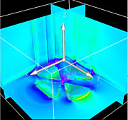
Schuck and his colleagues at the Molecular Foundry, the DOE Nanoscale Science Research Center located at Berkeley Lab, have engineered nanoscale color sorters, bowtie-shaped plasmonic devices that capture, filter and steer light, acting as antennas to focus and sort light in tiny spaces to a desired set of colors (energies).
Originally developed for detectors, the innovative imaging concept has now been extended to visualizing plasmonic fields at nanoscale resolution. By imaging fluorescence from gold within the bowtie, the team was able to glean the position of plasmonic modes—oscillations of charge that result in optical resonance—just a few nanometers apart.
“By shifting their structure by just a few nanometers, we can focus light at different positions inside the bowtie with remarkable certainty and predictability,” says team member Alex McLeod, an undergraduate working at the Foundry. McLeod has used open-source software developed at Massachusetts Institute of Technology to develop a web-based toolkit for imaging plasmonic devices, which is now available on the National Science Foundation’s Network for Computational Nanotechnology.[Paul Preuss, 510.486.6249,
paul_preuss@lbl.gov]