
- Number 429 |
- December 22, 2014
Crystal Solar and NREL team up to cut costs
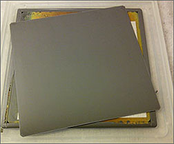
The monocrystalline silicon solar cells made
by Crystal Solar are much closer to true
squares than most other silicon solar cells.
The shape is one of the reasons the wafers
can be stacked vertically during the
gas-deposition process—and one of the
reasons that the cells can be produced at
about 100 times the typical rate.
Photo from Crystal Solar
A faster, cheaper way to manufacture silicon solar cells, partially funded by the Energy Department and fine-tuned at its National Renewable Energy Laboratory (NREL), has won a coveted R&D 100 award as a top technology innovation.
Crystal Solar's approach to growing high-quality, high-efficiency silicon wafers at 100 times the usual throughput and half the cost could be a game-changer, creating American jobs and stemming the flow of solar cell manufacturing overseas, says T.S. Ravi, chief executive officer of the Santa Clara, California-based company.
Even before he founded Crystal Solar, Ravi set a goal to speed up the manufacturing process. In 2011, his nascent company applied for the Energy Department's SunShot Initiative's Photovoltaic (PV) Incubator Program, which at that time was run out of NREL. The PV Incubator Program has a very competitive selection process, searching for ideas that are truly disruptive in terms of lowering costs.
"We applied for the program and were selected in late 2011," Ravi said, recalling a conversation he had several years ago with NREL's Harin Ullal. "I knew that if I could bunch a lot of wafers together, and find a way to remove the epitaxial wafer with a simple mechanical process, it could actually change the game in the solar industry."
Crystal Solar's direct gas-to-wafer method is epitaxial, which means it grows a layer of material on top of another material that has the same crystal structure. In the direct gas-to-wafer method—the official name is Direct Monocrystalline Silicon Wafer Growth by High-Throughput Epitaxy—gaseous layers of semiconducting silicon material are grown directly on reusable silicon substrates. The method has several advantages, including eliminating the waste incurred in the traditional approach, which involves sawing thin slices from a large ingot or block of silicon. In the new approach, wafers can be made thinner without compromising their quality or efficiency.
However, semiconductor material using the epitaxial approach typically grows very slowly—about two wafers an hour for the thickness needed for solar wafers. That's much too slow—and therefore costly—for solar cells.
Crystal Solar worked closely with NREL into 2013. "NREL pointed us in the right direction," Ravi said. "All these things we wanted to prove—that we could grow these wafers at a high growth rate, that we could do it without compromising the quality of the wafers—required the silicon defect expertise at NREL."
"We helped them understand the nature of the defects and thus improve performance at the wafer and cell level," said NREL Principal Scientist Bhushan Sopori, who, along with Ullal and NREL's Steve Johnston, worked with Crystal Solar on the process.
Ullal noted that the efficiency of the rapidly made cells is greater than 20% in the lab, so once in panels on rooftops, they should compare favorably to the best solar modules being installed today.
The new epitaxial system can produce up to 500 wafers per hour and sells for less than $5 million, while replacing traditional reactors and pullers. That translates to a wafer cost of about 13 cents per watt, less than half the typical cost of 30 cents per watt for high-end wafers, Ravi said. The entire module cost is projected to be less than 50 cents per watt—a reduction that could help nudge the installed cost of the solar system to less than $1 per watt.
Crystalline silicon commands 90% of the solar market, and despite the rapid success of thin films and other materials such as perovskite, will likely remain the leading technology in the near future.
Interest in the solar cells is huge, Ravi said. Crystal Solar is in the pilot manufacturing stage, and "we're struggling to keep up with the people who want our wafers. We want to set up a factory in the United States somewhere."
Ravi said the process lends itself to automation, which means labor costs—much cheaper in Asia—won't be such a big factor.
"We believe this technology will probably thrive in the United States, that it will be cheaper to do it here than anywhere else in the world," Ravi said. If the process continues to make high-quality efficient solar cells when ramped up to full manufacturing scale, it's a testimonial to the partnership between Crystal Solar, the Energy Department, and NREL, Ravi said.
The approach is cheaper and faster because it eliminates several steps, Ullal said. The device is actually built as gaseous silicon is deposited on a solid silicon substrate. A dopant or impurity can create the junctions that force current flow much more easily than in traditional solar cell manufacturing, Ravi said.
Another advantage: The material doesn't have to be rotated as it does in the ingot-growth process, which means the wafer remains a true square—and that makes for better and more efficient packaging of the PV module.
The approach also incorporates less oxygen in the silicon layer, which has been shown to eliminate oxygen-related defects. That's important because it gives the photons that hit the cells a tiny bit longer to form into the electron-hole pairs that are essential to establishing a carrying current for electricity, and makes it less likely that the electron and hole will recombine. The difference is tiny—1.3 milliseconds versus a bit less than 1 millisecond—but crucial in the world of photons and electrons.
"Most silicon wafers are made in Asia," Ullal said. "But this epitaxy process gets you there. And 30% of the overall cost of a solar module is the cost of the silicon wafer."
Typically, for epitaxial growth, wafers are arranged horizontally as layers are added. Crystal Solar arranges them vertically, for a smaller footprint, and passes the gas through a narrower space for a much higher growth rate.
"The key challenge was how to hold that wafer vertically and still get uniformity," Ravi said. "That took us 2 and a half years of researching for just the right material, the right shape, and so forth. There are so many advantages of the epitaxial method that it seems like a no-brainer. But the reason no one has really done it before is that it is a very hard thing to do in practice."
Learn more about NREL's photovoltaic research.[Bill Scanlon, 303.275.4051,
william.scanlon@nrel.gov]